
Discover how EMC issues can occur at the PCB level and by using simple layout techniques these can be resolved.
Electromagnetic Interference (EMI) is a significant issue in modern electronic circuits. Problems with electromagnetic compatibility (EMC) in the printed circuit board (PCB) design are often responsible for re-design cycles. While it is impossible to eliminate EMI, we can make our PCB design less vulnerable to EMI [1].
1) Potential EMI sources
At the PCB level, various potential sources of interference can cause multiple potential threats/effects. Some of these include conducted & radiated EM emission and electrostatic discharge (ESD). Conducted disturbance enters the system through power input lines and cables. In contrast, radiated disturbance happens due to EM waves from power & communication lines and switching devices. It propagates through electronic devices and traces through the air to interfere with other electronic systems [2]. On the other hand, ESD happens when there is an accumulation of positive or negative charges on insulators or unconnected conductors. This can damage the PCB and any electronic component soldered on the PCB [3].
Fig. 1 shows all the potential noise sources that can affect the PCB. The ribbon cable on a PCB connector can form an arm of a dipole, creating a parasitic antenna. Current and voltage peaks occurring during switching process of the active components in power supply can lead to excitation of this parasitic antenna, thus resulting in rise in the radiation pattern. Furthermore, the traces connecting the two ICs on the PCBs are connected with several 90 ° degree angles. If the ICs are switching at high frequencies, this arrangement can lead to ringing and crosstalk, thus, deteriorating the EMC performance.
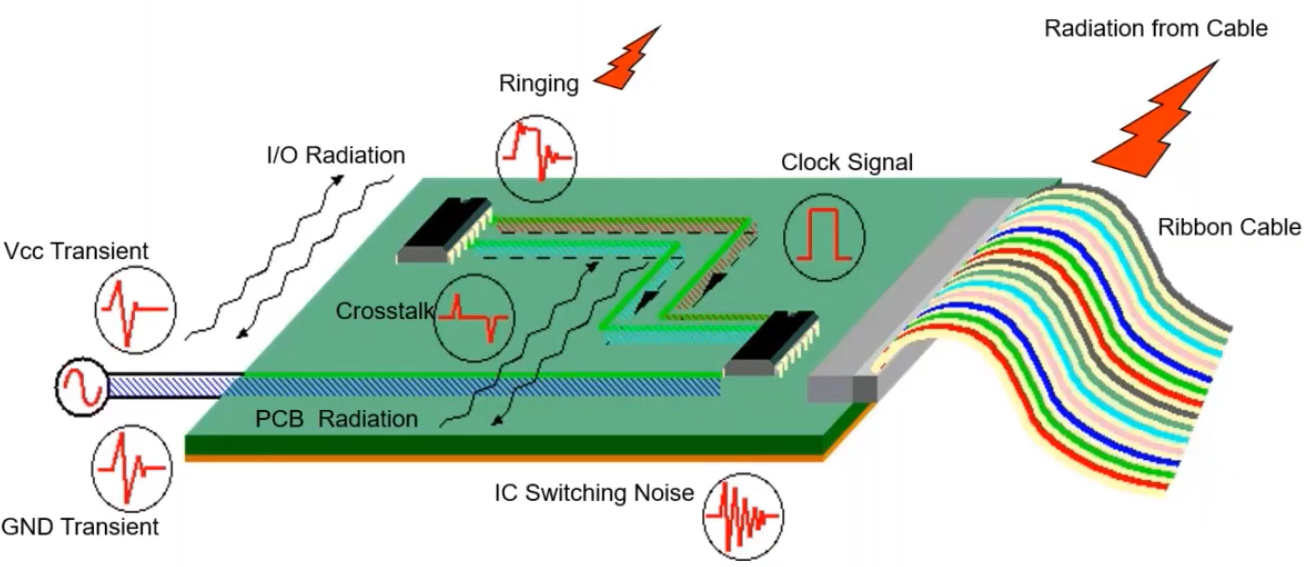
Fig. 1 Noise sources on a PCB
2) EMC compliance at the PCB level
To manage EMC in the design process and to detect problems at the beginning of the PCB design, one has to consider several aspects of compliance. Firstly, evaluating the parasitic antennas (electrical/magnetic monopole & dipole structures) that can form on a PCB is essential. One method to avoid radiation from these parasitic antennas is shielding. A mechanical shield, a closed conductive container connected to the ground, can be used to absorb most of the radiation from the loop antenna, protecting external interference and preventing data loss. Subsequently, one has to analyze the return paths and current loops. Longer paths can create a ground loop and form a radiating antenna. Therefore, PCB designers should keep the return paths as short as possible to reduce crosstalk [4].
ICs operating on PCBs and switching at a higher frequency can be one of the sources that introduce switching noise in the connected power rails. Decoupling capacitors should be placed near the IC power supply pins to reduce this conducted noise [5]. Additionally, using power planes instead of power supply traces can also minimize the power noise by creating a parallel plate decoupling capacitor between itself and the ground. Another potential EMC problem that needs to be resolved is impedance matching. Ringing and signal reflections occur when the impedance between source and sink is not adequately controlled/matched. Signal termination strategies can be used to slow down the rising and falling edges of the transmitted signals. However, it is recommended to implement this at the IC level by optimizing the bill of materials (BOM) and IC space.
3) PCB layout techniques
Effective PCB layout techniques can be used to enhance EMC performance. Such techniques are low-cost since the PCB production costs are much lower than the components soldered on it. It is important to note that poor PCB layouts cause more EMC problems than they can cure, and adding other filters/components may not resolve the issue.
A) Segregation of sensitive components
For an EMC-compliant design, PCB components must be grouped according to their operating signals, such as analog, digital, power supply, etc. The signal traces for each component group should stay in their defined area. Fig. 2 illustrates how four different circuits can be separated using segmentation. The ground plane effectively isolates the circuits using unmetallized moats/channels. The inductors and capacitors filter each circuit, and the coupling between power planes decreases [6].
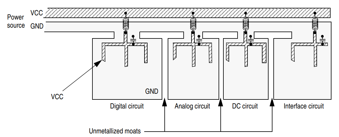
Fig. 2 Segmented functional blocks
B) Separation of traces
Trace separation minimizes crosstalk and electromagnetic coupling between adjacent/parallel traces on the same or different PCB layers. The general rule states that the separation between traces (measured between center to center) should be greater than or equal to 3 x trace width (Fig. 3). Larger the separation, the lower the crosstalk and coupling.
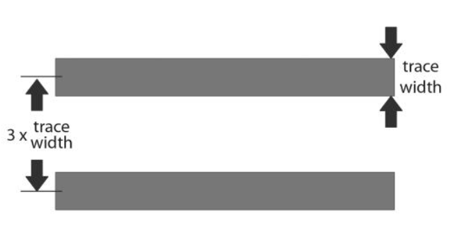
Fig. 3 Trace separation
All traces usually routed on the same layer are microstrip lines. That is a planar transmission line placed on top of a ground plane. They can transmit signals from DC up to high frequencies. For specific cases where a higher number of parallel traces are required on the same layer of the PCB with minimum separation, a co-planar waveguide (CPW) can be used. For example, the grounded CPW increases the amount of ground around a circuit compared to a microstrip by placing ground planes on the bottom of the dielectric material and the same plane, ensuring that the ground plane extends continuously on both sides of the signal transmission lines. It can minimize the crosstalk between the signal traces on different layers of the PCB [7].
C) Traces layout techniques
Vias are used in multi-layer PCBs for signal routing purposes. If not appropriately designed, some vias can introduce a parasitic capacitance and inductance effect. Such vias should be avoided and placed as far as possible from critical traces. Because of the parasitic capacitance and inductance in the vias, there is an impedance mismatch between via and trace, which creates reflections [5]. When vias cannot be avoided, it should be made sure that the ground vias should be placed close to the signal vias. This arrangement reduces the change in the characteristic impedance value and hence reflections.
Similar to vias, right-angled 90° track turns should not be implemented since it increases the parasitic capacitance, leading to a change in the characteristic impedance, resulting in reflections. As shown in Fig. 4, all orthogonal tracks should adopt a 45° bend to limit the noise coupled to nearby traces.
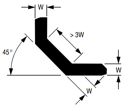
Fig. 4 Angled trace at 45°, where W is the trace width
The width of a signal trace should be constant from source to load. Varying a trace’s width creates impedance changes (resistance, inductance, & capacitance) and, therefore, causes reflections in case of high-speed signals and line impedance imbalances. In addition, split apertures (i.e., wide vias or long holes) in power and ground planes should be minimized as they create an area of non-uniformity within the planes. This leads to a reduction in shielding effectiveness and an increase in overall impedance [6].
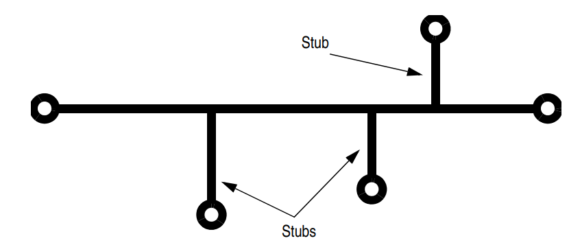
Fig. 5 Stub traces
Stubs produce reflections and the potential of adding wavelength divisible aerials to the circuit. Although a stub length may be a non-quarter wavelength integer of any known signal in the system, incident radiated EM waves may resonate on a stub (Fig. 5). Therefore, stubs with traces carrying high frequency or sensitive signals should be avoided while routing [6].
D) Arrangement of PCB layers
EMC performance of a PCB also depends upon the arrangement of its layers. In the case of a 2-layered PCB, one entire layer should be used as a ground plane. If an entire layer of ground is impossible, then ground grids should be placed. For a 4-layered PCB, the layer below the ground layer should be used as a power plane [8]. PCBs with more than 4 layers should have an even number of layers and consist of alternate ground and signal layers to avoid EMC issues. Fig. 5 shows the stack-up for FR4 1.6 mm 4-layered PCB built around a core (laminate). The core is a thick dielectric sheet with copper layers on both sides. The top and below of the core are added with thin prepregs, i.e., dielectric material sheets. For this specific case, Midlayer 1 and 2 represent the ground & power planes, respectively. The top and bottom layers are utilized as signal planes, and several components can be soldered on each side. The configuration of multi-layer stackup plays a critical role in EMC applications.
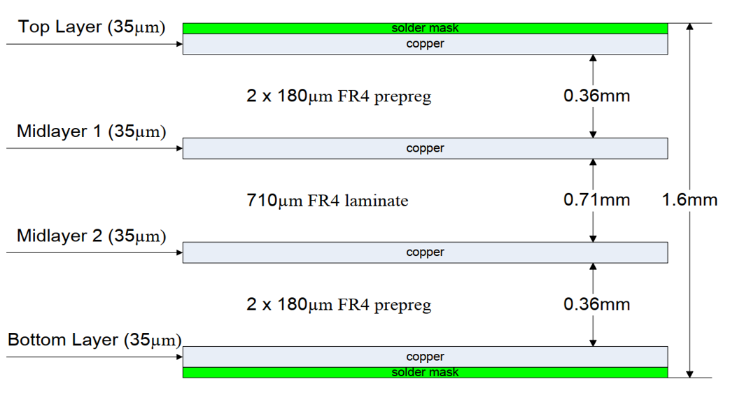
Fig. 5 PCB layers stackup
Conclusion
The above blog highlights the general PCB design guidelines for an electronic product or system, which can help reduce the effect of EMI. Better EMC performance can only be achieved when the designer knows the potential EM threats, understands the importance of mitigating them early in the design phase and eliminates the EMI from the system. The goal is to maintain the circuit board’s intended functionality to characterize the device under test effectively.
References
[1] D. Sharma and G. Vanga, “PCB design guidelines of Smartphones and Tablets for EMC,” in Proc. Int. Conf. Electromagn. Interfer. Compat. (INCEMIC), pp. 1-3, 2016.[2] M. Huang and J. Dai, “PCB layout modification to change the noise transfer path,” in Proc. IEEE 5th Int. Symp. Electromagn. Compat. (EMC-Beijing), pp. 1-3, 2017.
[3] System Design and Layout Techniques for Noise Reduction in MCU-Based Systems, Freescale Application Note, AN1259.
[4] EMC at Component and PCB Level, Martin O’Hara, Newnes, 1998.
[5] Printed Circuit Board Design Techniques for EMC Compliance, Mark I. Montrose, IEEE press series, 2000.
[6] A. Weiler and A. Pakosta, “High-speed layout guidelines,” Texas Instruments, Tech. Rep., 2006.
[7] M. Koohestani, N. Pires, A. K. Skrivervik, and A. A. Moreira, “Bandwidth enhancement of a wearable UWB antenna near a human arm,” Microw. Opt. Technol. Lett., vol. 55, pp. 2965−2967, 2013.
[8] H. Pues and D. Pissoort, “Design of IEC 62132-4 compliant DPI test boards that work up to 2 GHz,” in Proc. Int. Symp. Electromagn. Compat. (EMC EUR.), pp. 1-4, 2012.
About the Author: Qazi Mashaal Khan
 Qazi Mashaal Khan finished his Master’s Degree in Smart Systems Integration with distinction in 2019. This was an EU funded Erasmus + Program where he spent his four semesters in UK, Norway, Hungary and Germany. The host was Heriot-Watt University, UK. For his master thesis, he was able to work on Ultra- High speed Analog to Digital Converters and test the transfer speeds using FPGAs. He finished his Bachelors in Electrical Engineering from Fast NUCES Peshawar, Pakistan in 2016 with Summa Cum Laude. This was followed by a year as a Lab Engineer at his department, where he developed a passion for teaching.
![]()