
According to Market Research Future (MRFR) report, SOI (silicon on insulator) market is predicted to grow a lot by 2026 [1]. SOI is a key factor in different applications such as MEMS and sensors, power and RF components used in automotive, healthcare applications and internet of things (IOT).
The unique feature of SOI is a thin layer of insulator which separates the integrated-circuit structure from the bulk substrate. This leads to different benefits of silicon on insulator over bulk CMOS, which includes lower parasitic capacitance, latch up free behavior, higher package density and lower leakage currents [2]. From Fig. 1, the difference between these two technologies can be observed.
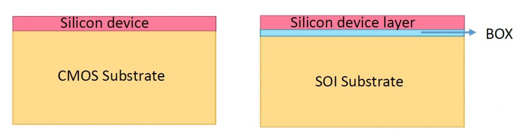
Fig. 1. Left: bulk CMOS substrate model. Right: SOI substrate model.
As shown in Fig. 1, the differences between SOI and CMOS technologies are fueled by different substrates, causing the transmitted noise through substrate (crosstalk) vary. It is well known that the daunting challenge in mixed-signal chip is to reside digital and analog circuitries on the same die, where the sensitive analog circuits can work in this noisy environment [3].
While bulk substrate with 10 Ω-cm can be modeled as a resistive medium for frequencies approximately below 15 GHz [4], SOI substrate modeling is another story because different simplified models are valid in limited frequency ranges. For more detail see Fig. 2 which shows the SOI substrate model w.r.t. crosstalk over different frequency ranges. Here the crosstalk is modeled by the scattering-parameter S21 between port 1 and port 2 in a SOI substrate. As it is shown in Fig. 2, S21 increases with a slope of 40 dB per decade which is due to two zeros created by the oxide layer capacitance, C1. As the frequency increases, a knee-point frequency, f1, can be observed which is dependent to oxide layer capacitance, C1, and the resistivity between the top and the bottom of the substrate, R2. At medium frequencies, the crosstalk in SOI can be modelled with the bulk resistive model. The increased crosstalk by a slope of 20 dB per decade at higher frequencies is due to the relaxation time of majority carries in the silicon substrate by C3. The capacitor C3 interacts with resistor R3 to show the coupling between port 1 and 2 through the air, silicon and oxide layers. They also create the second knee frequency point, f2. [5,6]
As a conclusion, studies show that using SOI technology has some benefits over bulk CMOS technology. According to discussion above, from a crosstalk point of view, SOI is a better candidate when compared to bulk CMOS at low frequencies, however, at higher frequencies, the crosstalk increases for both technologies. Hence, more investigation on this subject to decrease the coupling through the substrate is needed.
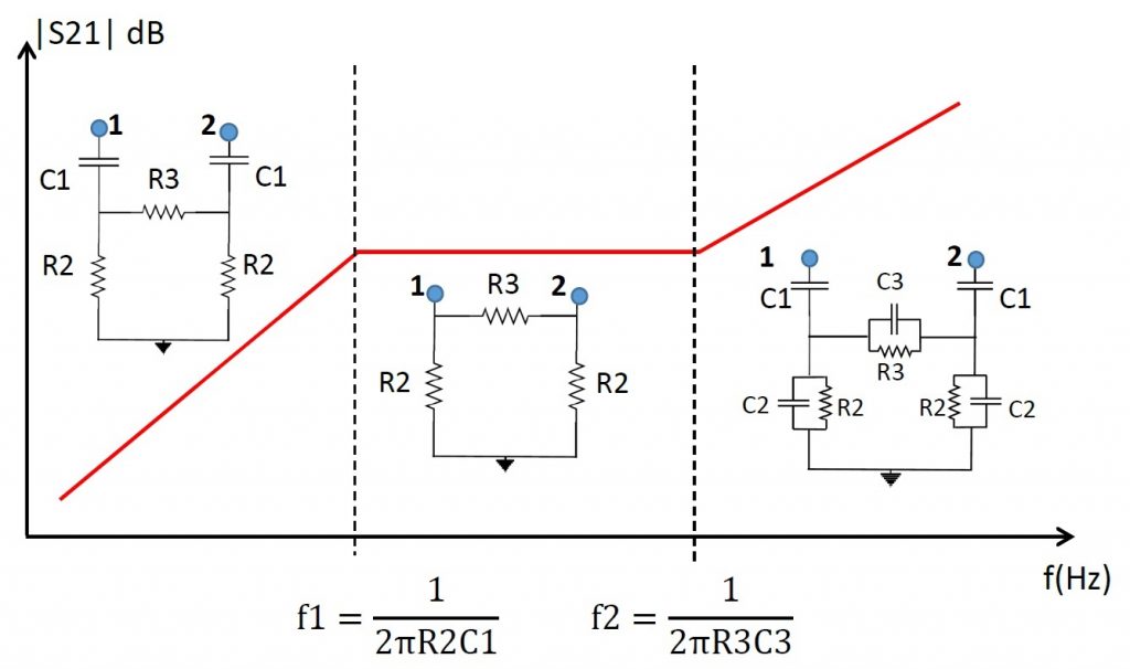
Fig. 2. Modelling the SOI substrate w.r.t. crosstalk over frequency [5,6].
References
[1] Future, Market Research (2021-02-17). “Silicon on Insulator (SoI) Market is Anticipated to Surpass USD 2.40 Billion By 2026 | APAC Region to Remain Forerunner in Global Silicon on Insulator Industry”. GlobeNewswire News Room. Retrieved 2021-03-07.[2] Silicon-on-insulator – SOI technology and ecosystem – Emerging SOI applications by Horacio Mendez, Executive Director of the SOI Industry Consortium, April 9, 2009
[3] L. M. Franca-Neto, P. Pardy, M. P. Ly, R. Rangel, S. Suthar, T. Syed, B. Bloechel, S. Lee, C. Burnett, D. Cho, D. Kau, A. Fazio, and K. Soumyanath, “Enabling high-performance mixed-signal system-on-achip (SoC) in high performance logic CMOS technology,” in Proc. Symp. VLSI Circuits Dig. Tech. Papers, 2002, pp. 164–167.
[4] Helmy, Ahmed, and Mohammed Ismail. Substrate noise coupling in RFICs. Springer Science & Business Media, 2008.
[5] Ankarcrona, Johan, et al. “Low resistivity SOI for substrate crosstalk reduction.” IEEE transactions on electron devices 52.8 (2005): 1920-1922.
[6] Raskin, J-P., et al. “Substrate crosstalk reduction using SOI technology.” IEEE Transactions on Electron Devices 44.12 (1997): 2252-2261.
About the Author: Akram Ramezani
 Akram Ramezani is an Early Stage Researcher in the EU MSCA-ETN PETER project. She is working on the ESR14 position “Risked-Based EMI-Aware Design of an Automotive Integrated Circuit”. She earned a Master’s degree in Electronic Engineering from Ferdowsi University of Mashhad (Iran, 2017). After graduation she has acquired practical experience in both the electronic and EMC field. Her goal in this project is to improve the design-for-EMC approach to include ageing and environmental stress factors and to increase the intrinsic EMC robustness of the chip by considering a “risk-based” approach.
![]()