
Career prospective of a PhD in Academia or Industry?
Secondments are an integral part of the MSCA ITN projects (PETER), enabling early-stage researchers (ESRs) to work in different institutions, receive exposure to state-of-the-art labs, achieve new skill sets, and collaborate with other researchers in a relevant industrial/academic environment. From 31st May to 30th July (2021), I took part in my first physical secondment at Melexis Technologies NV, located in Tessenderlo, Belgium. This was an eye-opening experience and led me to believe that the future of a Ph.D. graduate working in the industry is quite promising.
1) Organization and Commencement
At the PETER kick-off meeting, it was mutually decided between ESEO, Melexis, and the University of York that the secondment plans of ESR 7, 9 & 14 would be altered to ensure better collaboration towards their research. The secondment at Melexis was initially scheduled in 2020 but was delayed due to the Covid-19 pandemic. It was not feasible to carry it out virtually since measurements were required. Hence, the secondment was finally commenced from 31st May 2021. I reserved an apartment at Leuven, Belgium, and a carpool was organized by Melexis. Unfortunately, ESR 9 could not join physically due to visa issues and had to participate virtually.
During the first few weeks, the EMC team at Melexis was very hospitable, and I was given a detailed tour of their labs, including a Reverberation chamber, Bulk current injection (BCI), and Direct power injection setup, etc. The work environment was entirely professional, with full technical support by my secondment supervisor Dr. Hugo Pues. I was able to fit in quite well and started to develop a plan that could lead me closer to my research goals.
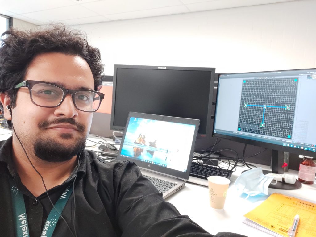
Fig. 1 My workplace at Melexis
2) Technical Work
The goal of my Doctorate is to develop behavioral models of EMC conducted immunity & emission considering the effect of Ageing at the integrated circuit (IC) Level. The primary focus of this secondment was to perform immunity measurements on a test chip developed by Melexis, which would help create an ICIM-CPI, integrated circuit immunity model- conducted pulse immunity. It consists of a pulse propagation network (PPN) that propagates transient pulse into the IC. This network represents linear effects with the passive distribution network (PDN) and the transient effects with the non-linear block (NLB). The model’s failure behavioral (FB) component will predict the failure modes due to overvoltage and overheating.
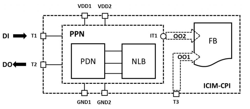
Fig. 2 Structure of an ICIM-CPI model
The suitable test chip selected was a dual output hall-effect latch & switch sensor in a TSOT23-5L package. The IC was considered to be a black box, and conducted immunity measurements were carried out. To protect an IC from internal damage, electrostatic discharge (ESD) protection devices are connected to its pins. To characterize these structures and quantify their robustness against ESD, the transmission line pulse (TLP) method is required to help model the NLB block. Increasing levels of current and voltage are applied until the component is destroyed. I designed a custom TLP, 4-layered printed circuit board (PCB) for the Melexis test chip for on-powered measurements. Since this is a destructive method, 15 samples of PCBs were tested (injection into the supply voltage) with different rise times, pulse widths, and voltage magnitudes up to 2.5 kV.
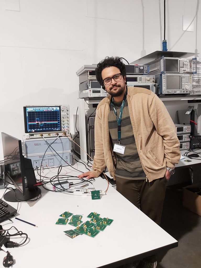
Fig. 3 TLP measurements (15 samples destroyed! )
To create the model’s FB block, DPI measurements must characterize the failure modes (hard failure, soft failure). DPI is an EMI immunity test for ICs, where RF disturbance is injected into the IC under test, and the forward power of the injected signal is increased until the functionality of the circuit fails according to a failure criterion. The frequency range of the RF disturbance is between 150 kHz and 1 GHz. A custom DPI board (made by Melexis) with on-board bias-tees was tested with power levels from 0 dBm to 37 dBm. The failure criteria selected were a 10 % deviation in the output voltage and the supply current. Help and support were provided by Hugo and Akram Ramezani (ESR 14, Melexis) to configure the test setup and monitor the results.
Fig. 4 DPI test bench
The last part of the model, PDN, required developing the S-parameter (Scattering) PCB, which was unavailable at Melexis. Due to lack of time, this task was given to Arunkumar (ESR 9, York), who virtually designed the test board, which is currently in the fabrication phase. After this, I will have all the necessary tools and data to create an ICIM-CPI model, including the effect of Ageing.
3) Collaboration
During the secondment, Akram and I collaborated on two research conference papers successfully submitted to EMC Compo 2022. Our ESEO and Melexis supervisors provided fruitful discussions that led us to analyze and explain our results effectively. We both have a clearer image of our P.hD objectives now and will continue to work together in the future. The papers mentioned are the following :
- A Comparison among DPI immunities of Multi-stage CSVCOs and Ring Oscillators (first author: Qazi Mashaal Khan, co-author: Akram Ramezani)
- A new TRL/TRM PCB-based Calibration Method for On-Board Devices Under Test (DUTs) (first author: Akram Ramezani, co-author: Qazi Mashaak Khan)
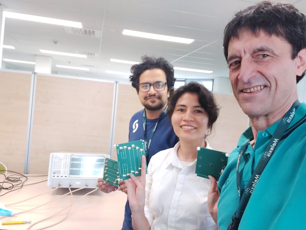
Fig. 5 S-parameter measurements using a 4-port VNA (TRM/TRL calibration method)
4) Prospective of a Ph.D. in Industry
One of the most significant decisions researchers face is choosing whether to pursue a career in industry or academia. While this decision is easy for some, it can be incredibly challenging for others. Before starting my MSCA ITN PETER doctorate, I had the concept that companies do not want to hire PhDs because they are overqualified and too independent. I aimed to stay in academia and become a full-time professor since I had a passion for teaching. Although I was already familiar with scientific work at the university, but not with everyday life in a company. After my secondment at Melexis, I explored the prospect of PhDs in industry and found out that the demand for highly qualified researchers has increased considerably in the past few years. A Ph.D. holder is well suited to help companies maintain and build an innovative culture. The scope of work is typically focused on applied research that will have direct clinical value. I learned that industry work also requires a more business-minded approach, as one has to develop projects that support the company’s business plan.
Time in a company’s research & development lab is more structured than academia and typically revolves around a standard 9-to-5 workday. Researchers are working towards a more critical, shared goal in industry and can collaborate as a team. The pressures are more deadline-driven, as teams work to integrate science and business-focused problem solving on tight project timelines in accordance with more extensive product and business goals. Another benefit of working in the industry is higher salaries and state-of-the-art resources being supplied by larger organizations. One also has the opportunity to climb the organizational ladder to manage bigger teams. After re-analyzing my strengths, I have realized that I have the required skills to transition into the industry in the coming future.
To conclude, I consider myself lucky and honored to be part of the MSCA ITN PETER consortium, which provided me the opportunity to work in the industry and collaborate with other fellow researchers. I would recommend my fellow ESRs and (other MSCA projects researchers) never to opt for virtual secondments unless they are necessary. A physical secondment allows you to experience the culture of a new country, work in a different environment, broaden your horizons, and conduct innovative research.
About the Author: Qazi Mashaal Khan
 Qazi Mashaal Khan finished his Master’s Degree in Smart Systems Integration with distinction in 2019. This was an EU funded Erasmus + Program where he spent his four semesters in UK, Norway, Hungary and Germany. The host was Heriot-Watt University, UK. For his master thesis, he was able to work on Ultra- High speed Analog to Digital Converters and test the transfer speeds using FPGAs. He finished his Bachelors in Electrical Engineering from Fast NUCES Peshawar, Pakistan in 2016 with Summa Cum Laude. This was followed by a year as a Lab Engineer at his department, where he developed a passion for teaching.
![]()